|
|
|
   |
|
|
|
|
I designed this computer to be somewhere between the C64 and the Amiga home computers. The capabilities are somewhere around the late 80's to early 90's. It is an 8-bit computer with 2D graphics (no 3D drawing in hardware, but a reasonable software solution is possible). It offers 2D character maps and hardware sprites as the primary forms of graphics. It also has an 8 voice sound chip. Both the video and audio chips are also designed and implemented entirely by me.
This project is the result of about 3 years of my free time, which included learning the art of FPGA programming (implementing custom chip designs, and programming them into special devices that can execute those designs as if they were real hardware), as well as implementing the firmware code for core features such as keyboard, mouse and joystick support, SDCARD access, BIOS code, and the entire tool-chain back-end on the PC that are required to support programming for this computer.
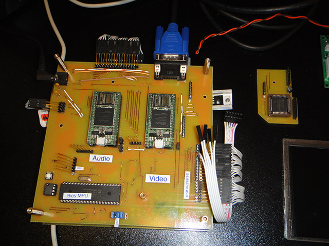
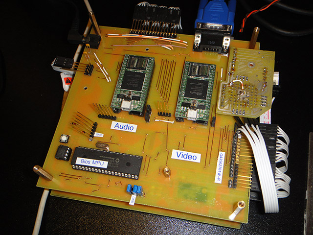
From the start, I wanted to ensure that the design of the computer was simple enough that anyone who can etch PCB's as a hobby, could make this computer as well. So I specifically designed for a single-sided PCB that could be etched and built at home, using typical home hobby-quality construction. I limited the board to 6x6 inches in size, so that a typical Pyrex baking dish could be used for the etching process. 6x6 isn't enough space for the entire computer, so I designed it to be two boards of this size. First, a main board of 6x6 inches in size with the Z80, RAM, address decoding and power supply. And second, another 6x6 inch board which sits on top of the first, containing the video and audio circuitry and a BIOS MPU which manages resetting and loading the computer with a program. Finally, on top of that board, is a smaller "daughter board" that offers the I/O interfaces like Keyboard, mouse, joysticks and SDCARD.
At this point, I must declare the usual butt-protections: This is a hobby-grade design, it may be full of horrible errors that damage equipment for all I know. If you choose to follow any of the design details that I show, or try any of this out for yourself, then you are fully responsible for your own actions. I cannot be held responsible for any resulting damage, errors or omissions. What else can I say.
This is not intended to be a step-by-step how-to build. This project would require a book to describe how everything works in detail. It's more of a general discussion regarding the design as it stands at the time of this writing. It will not likely be updated even if I do find more errors in the design. I am providing it purely to satisfy your curiosity.
The current build can be seen in action below.
The display is a 4096 color image @ 320 x 240 pixels (and is scan-doubled by the video-chip to 640x480 pixels for the VGA signal to the actual monitor). The refresh rate is 72Hz. I chose not to go with 60Hz because I am producing a VGA signal and 640x480@60Hz was not recognized as a standard resolution by my LCD monitor.
In case you are wondering, I eventually named it the Gremlin because I had to deal with quite a number of gremlins (I'd call them "rrrrrreally big bugs") throughout the implementation and debugging of the computer. But at this point, it seems to be operating as quite a rock-solid design, which is why I'm finally publishing some details about it.
|
|
|
|
|
|
|
|
|
|
|
|
|
|
My custom chips (video and audio) can be created at home, thanks to the humble FPGA chip.
An FPGA chip offers the hobbyist the ability to design any kind of chip they want (You must represent it as either a schematic, or as a special kind of code: Verilog, or VHDL are both supported). I tried using the schematic mode first, since I know how to create them. As it turns out (apparently), schematic mode is only offered for the dinosaurs of the electronics people out there now. It doesn't work very well (it can be difficult to refactor your design). Ultimately, I started to learn Verilog. It didn't take long to realize the benefits, and to convert my schematics to Verilog and ditch them. I choose Verilog, since it was easier to learn (it looked more familiar to me than VHDL), given that my background is C/C++.
The Xilinx tool-chain compiles this information for quite a while, then finally a chip definition file pops out! (or a bunch of errors, depending on your skill). Upload this chip definition file into the FPGA using a USB cable, and just like magic, you have the chip that you designed!
I used two XuLA 200's initially, then eventually upgraded to two XuLA2-LX25's which offered more internal RAM and capacity for larger logic designs.I chose to use the chips developed by Xess, because it made working with an FPGA easier in a few key ways: The pin spacing is easier to work with than would be possible with the physical FPGA chip itself, and the guys at Xess created some really easy to use tools to program the devices via USB cable.
These FPGAs are theoretically capable of operating at upwards of 300Mhz, and they are essentially massively parallel processing devices. However, we're not writing code for a CPU to run. We're writing state machine definitions, input/output logic, and pin descriptions which define the internal behavior of a chip.
When you program an FPGA, you are actually programming a small flash chip which the FPGA reads on power-up. Therefore, each time you apply power to an FPGA, it takes a moment before it becomes operational. My computer can deal with this because it has that microcontroller I call the BIOS, which is actually in control of when the rest of the computer comes out of reset. It waits a moment for the FPGA's to become ready after power-up, then begins copying data into memory, and finally releases the Z80 CPU from reset.
A CPLD is like a mini FPGA. It costs only about $2.00, vs. the FPGA's $60.00 or more. However, a CPLD can only hold a few tiny equations. The CPLD that I chose, also has a pinout that is well suited to homebrew PCB's. A CPLD is programmed with the same language and same tools as the FPGA's. However, it does require a different programming device than the XuLA FPGA boards (called a JTAG programmer). Once programmed, a CPLD is ready to run as soon as power is applied. Unlike the FPGA, it does not load its' configuration on every power-up. It is ready to run instantly.
When I set out to build this computer, I had a few objectives in mind:
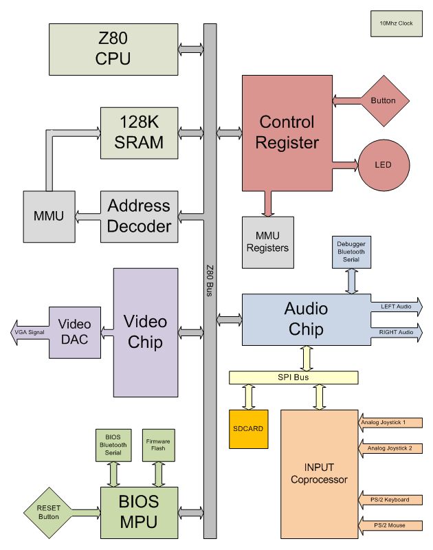
The above block diagram shows how there is one main bus (the Z80 bus), and one minor bus (the SPI bus). Most devices are on the main bus, and are thus directly accessible to the Z80. The Input Coprocessor is only accessible through the Audio chip (more on that later).
The 128K of SRAM is accessible through the Z80 bus, but some address translation occurs within the Address Decoder and MMU before the SRAM sees it.
The Control Register is simply an 8-bit latch that the Z80 can both read and write. It includes the LED, the BUTTON, and the MMU registers (two 3-bit registers that control the memory configuration and selected RAM bank). With those registers, two things are controlled: 1) How much memory is unbanked vs. banked, and 2) Which bank of the 128K of RAM appears in the banked region of memory.
The Address Decoder is implemented within a CPLD. It contains the equations that examine the current address on the Z80 bus, and select the appropriate device so that communication can occur with it. It also contains the equations that implement the MMU behavior, given the values of the two small registers in the Control Register.
The BIOS MPU is a PIC Microcontroller that has access to the Z80 bus. It also has control over the Reset signal. Thus, the BIOS MPU has a very special ability: It can hold the Z80 in reset while it reads data from the Firmware Flash chip, and writes it onto the Z80 bus. In this way, the BIOS MPU actually has the ability to do anything that the Z80 CPU itself could do, although it is slower. The Firmware Flash chip contains a variable number of data blocks that have been uploaded via a Bluetooth Serial Port. Each data block has a header that indicates a destination address where the data should be stored, as well as the length of data to be transferred, followed by the data itself.
The BIOS MPU has the Bluetooth Serial Port attached to it. The device was found on DealExtreme for under $10.00. Worth every penny! With this, I can connect my PC to my computer, and upload new data to the Firmware Flash through the BIOS MPU, without the need for a cable, and since it's a flash chip, that data will survive a power cycle.
The BIOS MPU listens to a physical RESET button, but it also accepts a command by Serial, to reset as well.
Finally, the BIOS MPU proved to be an incredibly powerful debugging system as I was initially getting the computer to run, since it was able to control the Z80 bus, and was therefore able to simulate just about anything that the Z80 itself was supposed to be able to do. Thus, I could exercise the address and data bus, and the various peripherals, even though one or more of them was not working properly yet (often rendering the Z80 itself inoperable).
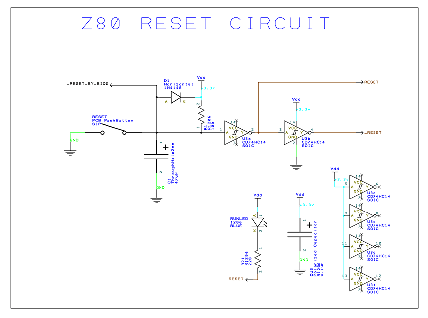
We'll start by looking at the reset circuit. It accepts two different inputs: One from a physical "Reset Button", and one called _RESET_BY_BIOS, which is an active-low signal from the BIOS MPU which is also capable of triggering a reset of the entire system. A resistor and capacitor work together (with some protection offered by a diode) to produce a minimum pulse width, regardless of the size of the input pulse. A Schmidt Inverter is used to clean up the pulse to be digital in nature again. This produces the RESET signal itself. Another inverter is then used, to produce the inverted version of the reset signal (_RESET). An LED indicates whether the Z80 is currently in reset. The remaining 4 inverters are unused, so their inputs are tied to a constant value. Finally, CU3 is the decoupling capacitor for the chip U3.

This shows how the Z80 itself is configured, and attached to the Z80 Bus. First, there are quite a few inputs to deal with: The /NMI is the highest priority interrupt source. It could be used as a hardware break button if desired, but I chose not to use it, so it's just tied high. The /INT is a more normal interrupt source. I do use this as my only interrupt source. This interrupt signal is generated by the video chip. There is a pull-up resistor here as well, in case the video chip is not currently connected, or not programmed correctly. The /RESET signal comes from the RESET block which I discussed above. I do not use the wait-state or bus ownership features, so the /BUSREQ and the /WAIT signals are pulled high. The clock source is injected into the Z80 here as well.
Finally, the Z80 Bus itself must be dealt with. It's made up of the following signals: 8 bits of Data (D0..D7 - thus, an 8-bit CPU), 16-bits of Address (A0..A15), and the Control signals /MREQ, /IOREQ, /RD, and /WR. With these signals, the Z80 is able to select any address, and read from or write to it. All of these signals are shared among most of the remaining devices of the computer. Because of this, I buffer all of these signals. Most of these buffers are configured to act as outputs only (i.e. Z80 -> Z80 Bus). Only the data bus is wired to switch directions, and it decides which direction based upon whether the Z80 wishes to read or write at the time. All of the buffers are also configured to "get off the bus" while the Z80 is held in reset. This will allow the BIOS MPU to take full control of the Z80 Bus while the Z80 is not running.
Note that the Z80 runs at 5v, while the rest of the computer runs at 3.3v. The buffers act as level translators, including the one for the data bus. The datasheet shows that, although the buffer only outputs about 3 volts for a high, the Z80 accepts anything over about 2.5v as a high, so it works perfectly fine. Additionally, the buffers are capable of accepting a signal as high as 5v even though they are running at 3.3v. I had to produce a spreadsheet that checked the various input and output voltages of every single chip in the design, to ensure that every chip can communicate with every other one. This was a huge pain in the butt, especially for the PIC chips, which seemed to be very non-standard. The FPGA's pins were actually programmable to behave like several different technologies so they were easy to deal with. These level translation issues caused me a lot of problems while troubleshooting the design, because I didn't fully realize how much of a problem it could be if the chips were not DESIGNED to work together. Bizarrely, the computer worked fine in the summer, but when winter came, that was enough drop in ambient temperature in the room to cause the computer to stop working. What a hair puller of a mystery that was. A lot of oscilloscope time was spent puzzling through that problem.
Regarding decoupling capacitors: Each chip gets its' own decoupling capacitor again, and the Z80 gets a tank capacitor as well.
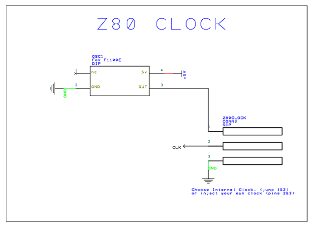
This small piece of the computer is responsible for producing the primary clock source. It's 10Mhz, as that's as fast as the DIP version of the Z80 can run. It also offers a way to inject your own synthesized clock source for debugging (through the 3-pin jack). Normally, a jumper sits across pins 1 and 2. Alternatively, you could connect a cable to pins 2 and 3 and produce an external clock of whatever speed you wanted.
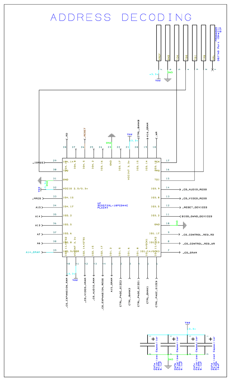
The purpose of the Address Decoder is to examine what address the Z80 is reading or writing to, and determine which device it intends to communicate with. It then informs that device, that it is the ONLY device that may pay attention to the Z80's transaction. All non-selected devices must close their eyes and cover their ears, and completely ignore whatever is going on on the address and data bus.
The Z80 has two address spaces: Main Memory (/MREQ), and I/O Memory (/IOREQ). Different devices are present in each address space, and at different addresses.
The port at the top of the diagram, is the JTAG interface for programming the CPLD itself.
The CPLD is an XC9572XL-10PCG44C. This device has lots of pins, and is perfect for implementing an address decoder and a tiny MMU all in one small package.
The CPLD can monitor the Z80 Bus activity, through the _RD, _WR, _MREQ, and _IOREQ signals. It can also see A13...A15, and A6...A7. Combined, these signals allow it to see whether a read or write is occurring, and to what block of memory.
By watching A6 , A7, and _IOREQ, the Address Decoder can recognize 4 I/O address block of 64 bytes each.
By watching A13 through A15, and _MREQ, the Address Decoder can recognize 8 RAM address blocks of 8K bytes each.
The top two blocks, C000-DFFF and E000-FFFF are the address regions for the Audio chip and Video chip, respectively. The address region from 0000-BFFF is entirely mapped to SRAM.
A collection of CS_xxxx signals are the Chip Select outputs. Each Chip Select signal controls a specific device. These signals are what tells a device to listen, or to cover its' eyes and ears and ignore the current memory transaction. Some devices offer main memory as well as I/O memory, so they get two Chip Select signals. The Control Register is made up of a Latch (which is write only), and a Buffer (which is read only and exposes the current latch values back to the Z80). Therefore, the Chip Select signals for this device are split into separate RD and WR signals.
There are a few EXPANSION signals which are unused at this time.
The MMU that I implemented is a very simple system that can remap blocks of SRAM by xor'ing the top 3 bits of the address that is given to the SRAM chip (A14_SRAM through A16_SRAM), thus shuffling blocks of memory around. The MMU is also given another 3 bit number which controls where in the main address space, a transition from unbanked to banked memory occurs. The unbanked memory region always sees block 0 memory. The banked memory region sees whatever block(s) or memory you have selected). Thus, you can configure the bottom of memory to have the code where ISR's and reset vectors live, and some mainline code. Then, you can configure an upper area of memory to contain a variety of libraries of code and/or data, which can be paged in when needed.
A14_SRAM through A16_SRAM are address signals that are generated by the MMU equations and offered to the SRAM chip. These equations are able to re-arrange the SRAM memory in blocks, and thus give the Z80 access to all parts of the 128K of SRAM in the SRAM chip. The CTRL_BANK0 through CTRL_BANK2 signals tell the MMU equations which bank of SRAM should be selected. The CTRL_PAGE_SIZE0 through CTRL_PAGE_SIZE2 signals tell the MMU equations how large the banked portion of memory should be.
This chip also manages a small portion of the RESET logic. Specifically, it can see when /RESET is asserted. It can also see when BIOS_OWNS_DEVICES is asserted. Basically, when the computer is reset, the BIOS MPU first causes a /RESET to occur. Thus, the Z80 goes into reset, and its' related buffer chips all go tristate. i.e. the Z80 is completely isolated from the rest of the computer. We want the Video and Audio chips to also enter reset now. However, we don't want them to stay in reset for very long. We want the BIOS_MPU to be able to load their VRAM and Sample memory with data, as well as push some memory into SRAM, all before releasing the Z80 from reset. So, another two signals are needed. BIOS_OWNS_DEVICES is a signal that the BIOS asserts shortly after reset begins. This is intended to indicate that, although the computer is in reset, we don't want certain devices to be resetting anymore. A second new signal is called _RESET_DEVICES. The devices which need to come out of reset early, will watch THIS reset signal rather than the traditional /RESET or RESET. The CPLD sees that /RESET is asserted, and decides whether to assert /RESET_DEVICES based on whether BIOS_OWNS_DEVICES. The BIOS MPU is now capable of taking the entire computer into RESET, then shortly afterwards, releasing only the devices from RESET. It can then load data into their memories, and finally, release the Z80 itself from RESET, allowing the computer to start executing code again.
The MMU can only rearrange the address space of the SRAM. It does not affect any other device.
I gave the CPLD 3 decoupling capacitors and one tank capacitor.
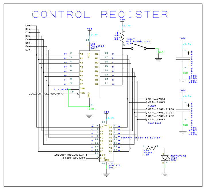
The Control Register is a single 8-bit register. It controls the MMU, and allows the CPU to read a button and light an LED.
It is implemented by using an 8-bit Latch to remember what the CPU last wrote to it, and a Buffer to allow the CPU to read what value the latch is currently holding. The Control Register is considered to be a Device by the BIOS MPU, so it responds not to the /RESET signal, but to the /RESET_DEVICES signal. So, the BIOS_MPU can reset it but it can also still control it while the Z80 itself remains in reset, thus allowing the BIOS_MPU to load the full 128K of memory before releasing the Z80 from reset.
The MMU related bits of the latched value are offered to the Address Decoder where the MMU implementation resides.
(NOTE: I think my LED might be drawn backwards)
Again, each chip gets its own decoupling capacitor.
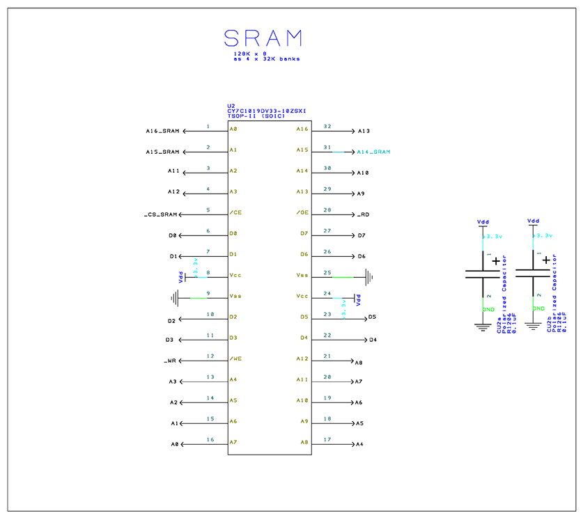
I chose this memory chip because it's very fast (10ns), and it has no need for refreshing (It's SRAM, not DRAM).
This chip simply needs to listen to the various signals of the Z80 Bus. The only unusual thing here is that the upper 3 bits of the Address Bus are produced by the Address Decoder and MMU.
The SRAM requires two decoupling capacitors.
This SRAM seems to be highly static sensitive. Try not to touch it or any related PCB traces.
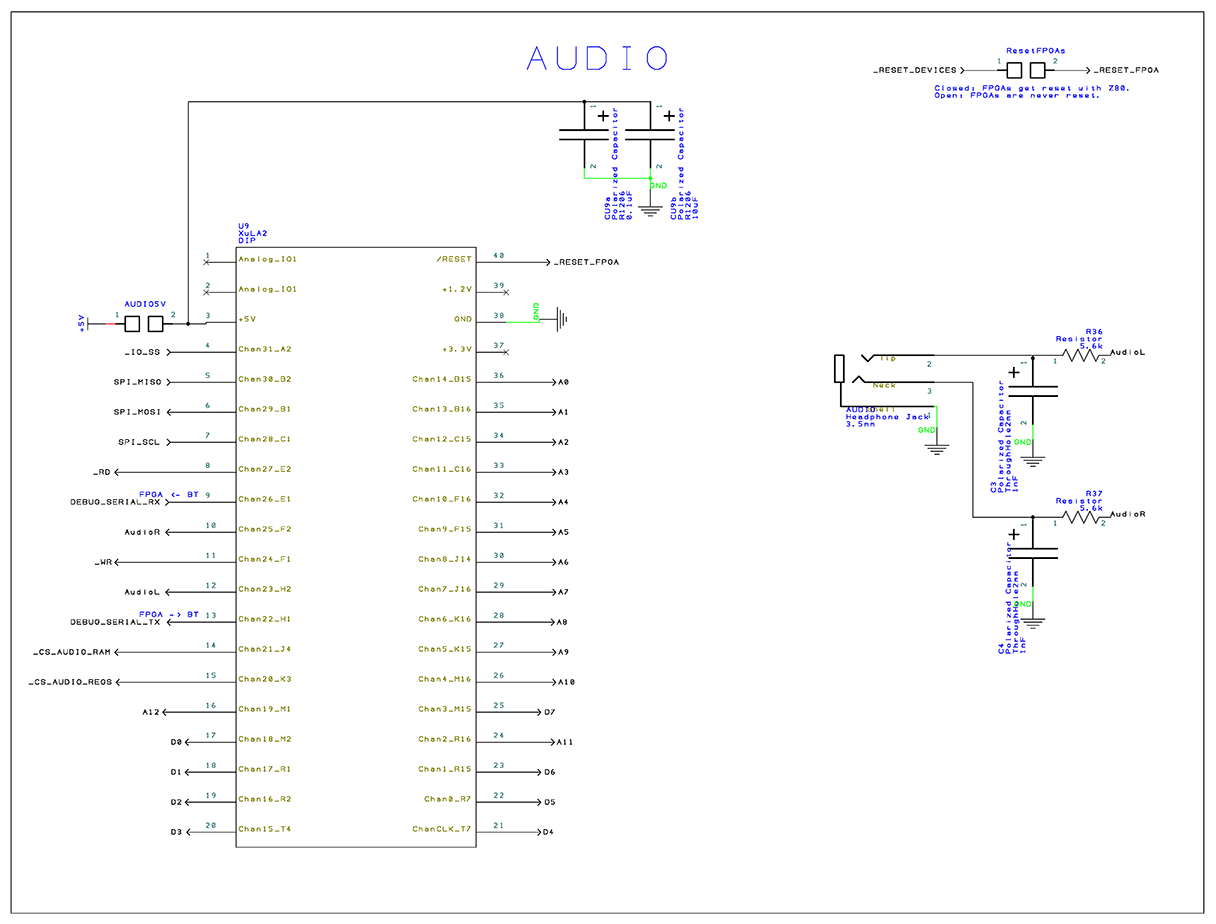
The Audio Chip is similar to the SRAM chip, with regards to which Z80 Bus signals it requires. No MMU signals though, since the Audio Chip's memory is not affected by the MMU. Only SRAM is. The Audio Chip does, however, offer memory in both the Main and I/O address spaces. Thus, it has two separate Chip Select signals.
A jumper is shown in the top right corner, which can be used to isolate both FPGA's (Video and Audio) from the rest of the system, so that they will survive a reset without themselves being reset. I've not found a real practical need for this yet. I just leave the jumper installed all the time.
Another jumper, seen on the left, controls whether the FPGA receives 5 volts from the system. This was offered, because the Xess FPGAs can be powered from their USB cables, in which case I don't want to create contention between the USB cable power and the onboard power regulators. I have since modified both of my FPGA's to require on-board power at all times (a simple cut of a specific trace as directed by Xess), and can therefore leave this jumper closed now.
A few new signals are seen here. There are the AudioL and AudioR signals exiting the audio chip, and passing through an RC filter before being offered to the audio jack. Each of these signals are called a "1-Bit DAC".
The Audio chip is also offering a simple Serial Port. Just the TX and RX signals are offered, no flow control.
Finally, the Audio Chip is connected as a slave on an SPI Bus (SPI_SCL, SPI_MOSI, SPI_MISO, and _IO_SS). This is how the Input Microcontroller gets its' data over to the Z80. The Audio Chip offers an 8K block of memory that the Z80 can write commands into, and read results from. The Input Coprocessor reads those commands, and produces results for the Z80 to see. There is a single COMMAND register that the Z80 can write to (inside the Audio Chip) that will trigger an SPI exchange to occur between the Audio Chip and the Input Microcontroller. There is also a RESULT register that the Z80 can check, to discover whether the results have been placed into memory and are ready for inspection. The Z80 is may poll this value whenever it wishes. This leaves the Z80 free to issue an input command, then do other things like game logic or rendering code while that command is executed and the data is transferred, then the Z80 can come back later and find the result. Or more simply, it could issue a command, and then poll in a spin-loop for the result to be set before continuing.
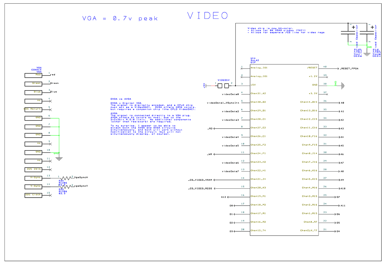
The Video Chip is very similar to the Audio Chip, with regards to what Z80 Bus signals it requires. The Video Chip also offers memory in both the Main and I/O address spaces. Thus, it has two separate Chip Select signals as well.
It also uses the same /RESET_FPGA signal that was shown in the Audio Chip schematic, as well as the same 5 volt jumper option.
Where the Video Chip differs, is with its' output pins. It offers videoData0 through videoData7. These 8 signals are routed to a header for a daughter card. The daughter card is responsible for producing the final video signal. That final video signal is then routed from the daughter card header, back to the VGA plug. This design allows me to create different daughter cards that accept the 8 bits of video data and produce a variety of different outputs. In fact, a daughter card could offer its' own output and not even bother to route the final results back to the VGA port (e.g. an X/Y plot). Of course, the Video chip needs to be designed to produce the appropriate data on those pins. But it's an FPGA, so yes, you can make it do whatever you want!

This is the simplest daughter card. No chips, just a few resistors. It treats the 8 bits of video data as 2 bits of red, 2 bits of green, 2 bits of blue, a VSync and an HSync signal. In this mode, there are 4 clocks per pixel occurring within the video chip. For all 4 clocks, the same values are output, so as to create a nice stable looking pixel. The Video Chip has an output stage which can be configured to produce data that is suitable for this simple setup. However, you are only seeing 64 colors out of the 4096 possible colors that the Video Chip is internally generating. Basically, you only get to see the top 2 bits of each color. This was the original design I used, while hoping to eventually think of a way to get all 4096 colors out of the chip. And then one day, I thought of.......
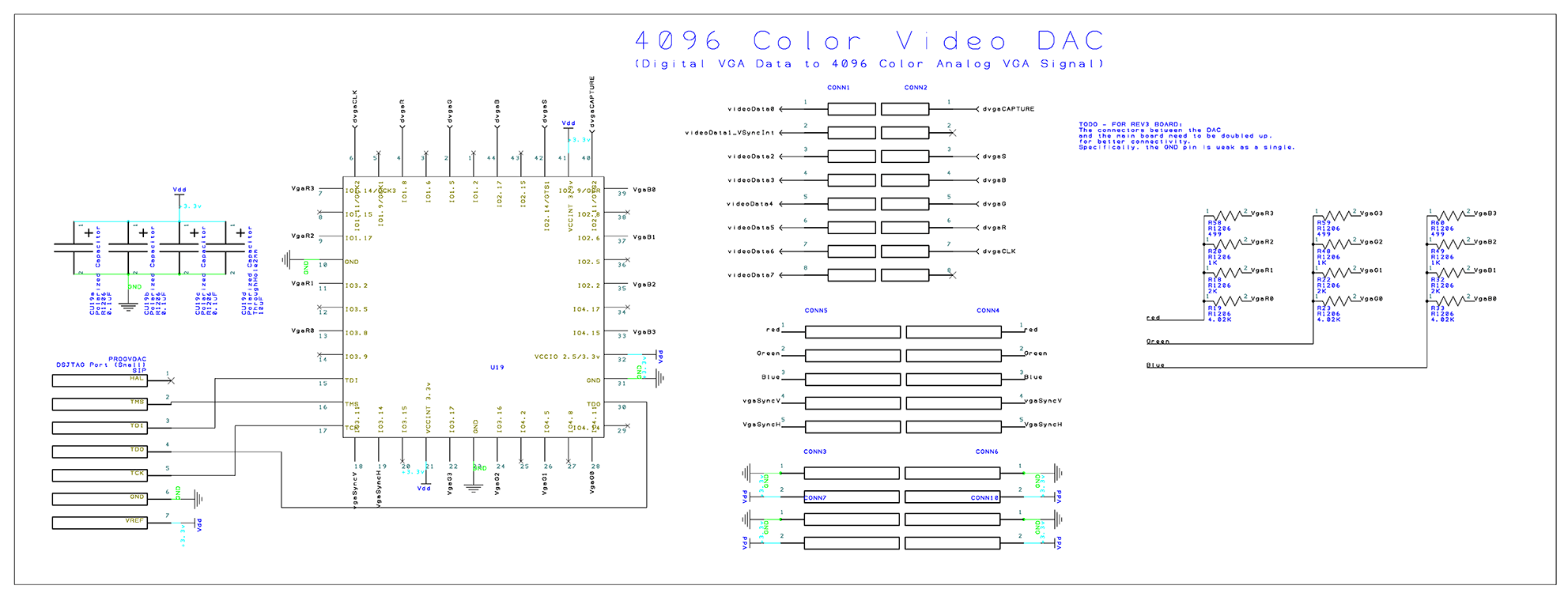
This daughter card features a CPLD configured with equations which make it become a "4096 Color Video DAC". It treats the 8 bits of video data as 1-bit of red, 1-bit of green, 1-bit of blue, a 1-bit Sync, a clock, and a capture signal. Each signal is running at the full 60Mhz that the video chip is internally operating. That gives me 4 clocks per pixel to get my work done. In those 4 clocks, I can output all 4 bits of color data on each 1-bit color pin. I also output the HBlank and the VBlank at specific moments on the Sync pin. The CPLD is collecting all of this data and building a full 4-bit red, green and blue color internally, along with the next state of each sync signal. On the final clock, the video chip outputs a high on the capture signal, indicating to the CPLD that the data for this pixel is complete. At that moment, all values are latched and presented as the next pixel of video data on the CPLD's output pins.
The Video Chip has an output stage which can be configured to produce data that is suitable for this daughter card as well. The result is a full spectrum of 4096 colors using this system.
One problem I had with this design, was not enough grounding. The connector which supplied the power and ground to the daughter card only offered one power and one ground pin, and that was not enough. I had to add additional grounding to stabilize the image. Offering a second ground pin solved the problem. With 60Mhz passing through this connection, I should have doubled or tripled-up most of these signals, I guess.
This Daughter Card system could be used to extend the computer's video output to generate several other types of video, such as:
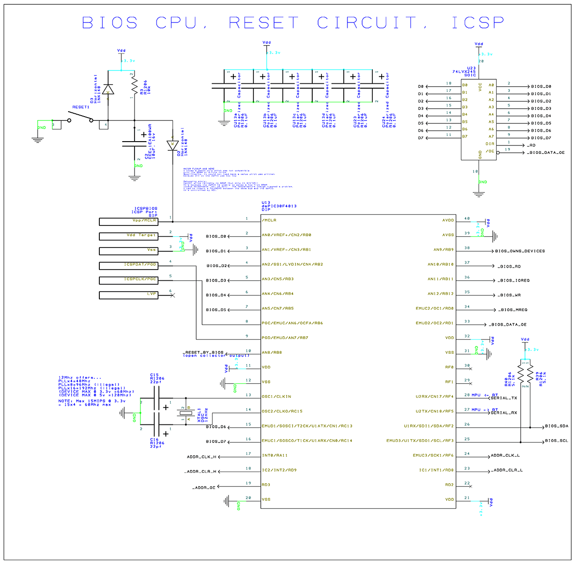
I had trouble deciding upon a good name for the BIOS MPU. It's not a BIOS in the traditional sense that a PC uses that term for. However, it is the simplest of ways that I get stuff (programs and data) into this computer, so ultimately, the name stuck.
The BIOS MPU has its' own RESET circuit, which is actually the primary way to reset the entire computer. When the BIOS MPU starts up, it forces the Z80 into reset as well, through the assertion of the _RESET_BY_BIOS signal. If you want to know more about how it resets all of the devices and the Z80, it's all described above in the section about the Reset circuit.
Unfortunately, this MPU chip is not electrically compatible with the rest of the system (hi and low signal voltages are not within spec). I didn't discover this until well into the debugging phase of the computer. I had already written quite a bit of the code for this chip, and didn't want to move away from it anymore. So, some buffer chips were necessary to fix-up the signal levels. U23 takes care of the data bus, and U24 (next schematic) takes care of additional Z80 Bus signals.
The address bus has its own problem: Even with 40 pins on this MPU, there are not enough pins to drive the address bus (it's 16-bit, and thus requires 16 pins!) Typically, bytes will be loaded from flash into Z80 memory in sequential order. Thus, it's possible to use two 8-bit counters to generate the address bus values. More on this later, in the BIOS Address Generation section.
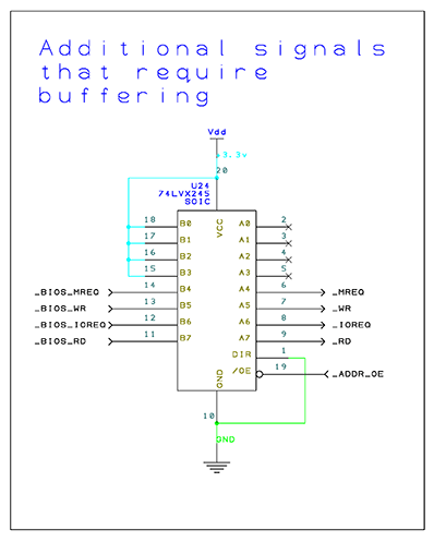
These are the additional Z80 Bus signals that required buffering.
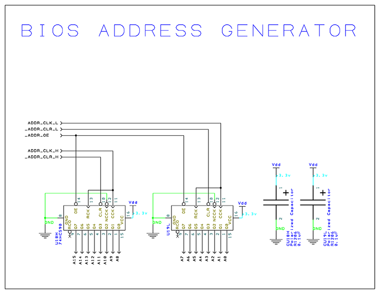
This is the address generation that the BIOS MPU uses. By using only 5 pins on the BIOS MPU, I am able to generate any 16-bit address and (more often than not) I can update it to the next desired address very quickly. Just toggle a pin to increment by 1. If I need to jump to a non-sequential address, I first reset the counters, then increment them up to the desired values again. By NOT chaining these two counters together, I can actually reach my desired address value much faster. With this configuration, I can increment by 1's or by 256's. Essentially, the low and high byte of the addresses are individually accessible.
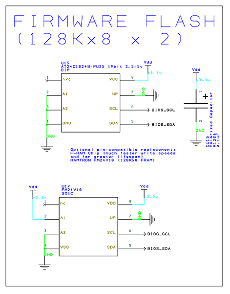
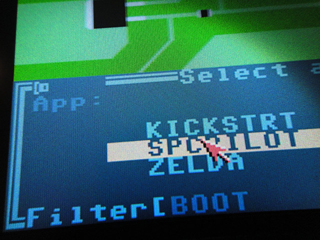
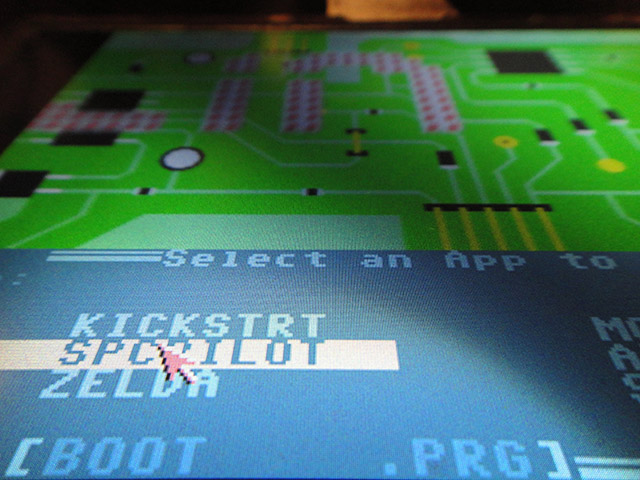
This is the chip that holds the initial code and data that is loaded into memory by the BIOS MPU just before the Z80 is brought out of reset. It used to contain all sorts of programs that I wanted to test, but now it usually contains a small boot-strap program that launches an app off an SDCARD that has been inserted into the computer. Although there are spots available for two chips, I've only ever needed to install one.
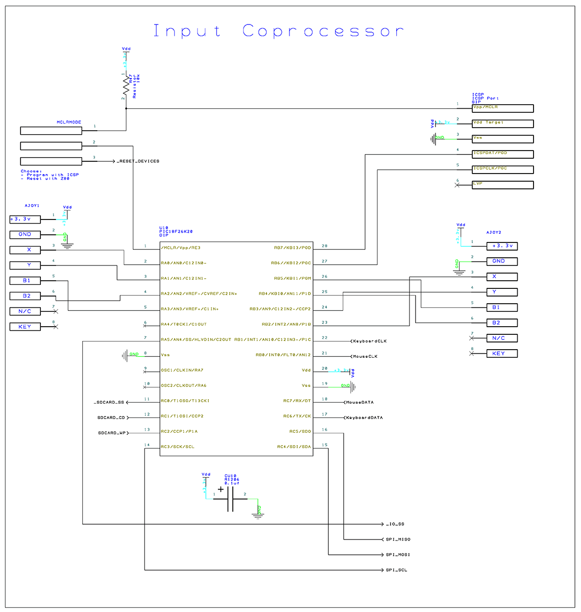
Here is the core implementation of the Input Board. In the top-left corner, is a 3-pin jumper. In one configuration, it allows the MPU to be programmed via ICSP. In the other configuration (the default configuration), the Input MPU will reset when _RESET_DEVICES is asserted.
There are two joystick ports, each with an analog X and Y axis, and 2 buttons each.
Two pins are all that's needed for Keyboard support. Likewise for Mouse, only 2 more pins are needed.
Input MPU is the master of the SPI bus, and determines when to talk to the Audio Chip and the SDCARD.
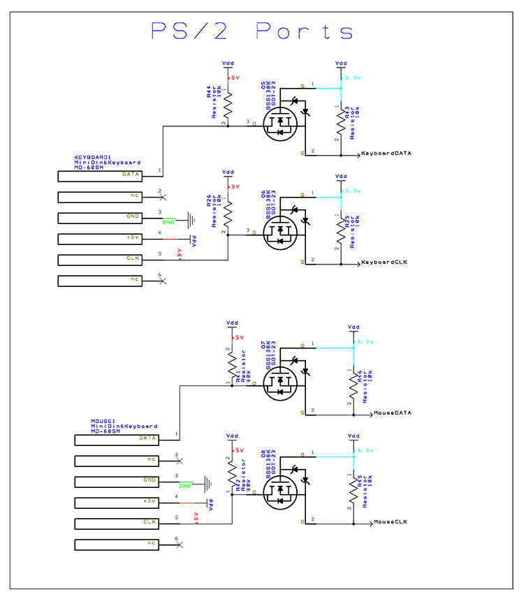
The PS/2 ports are 5 volt devices, but the Input MPU is running at 3.3 volts. Thus, we have another situation where level translation is necessary. The circuit may look unusual, but it's actually using a tiny FET and a couple resistors to create a 1-bit bi-directional level translation (and I repeat it 4 times). This is SUCH a handy little piece of circuitry that I found on the web somewhere long ago, and has come in handy so often in my designs! It might look a bit scary due to the FET diagram if you're a digital guy like me, but build it and it just works like magic.
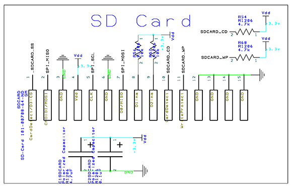
The SDCARD is connected to the SPI Bus, as well as the Input MPU. There is detection for "Card Presence" as well as "Write Protect". The SDCARD is operated in SPI mode.
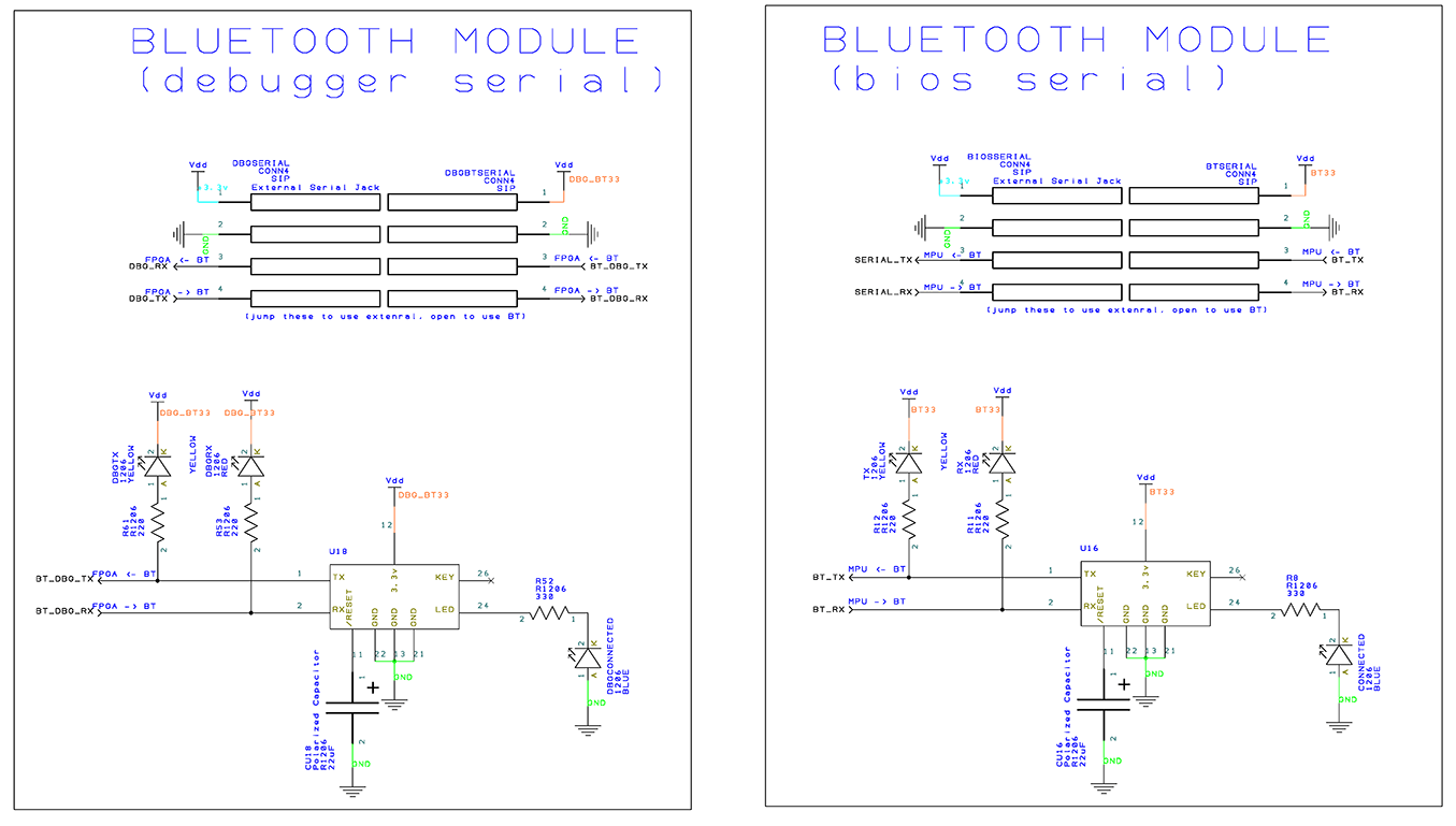
The two serial ports present in this computer are connected to small Bluetooth modules found on the website, DealExtreme. These Bluetooth Serial modules are very easy to use, and eliminate the need for a physical connection between my PC and this computer. One port controls the BIOS MPU, and thus allows for the uploading of data into Flash. The other one is directly accessible by the Z80 CPU (through the Audio Chip's address space), and is thus useful as a debugging interface.
Note that there is a header available for each port, which could be used to connect a wired serial interface instead, if desired.
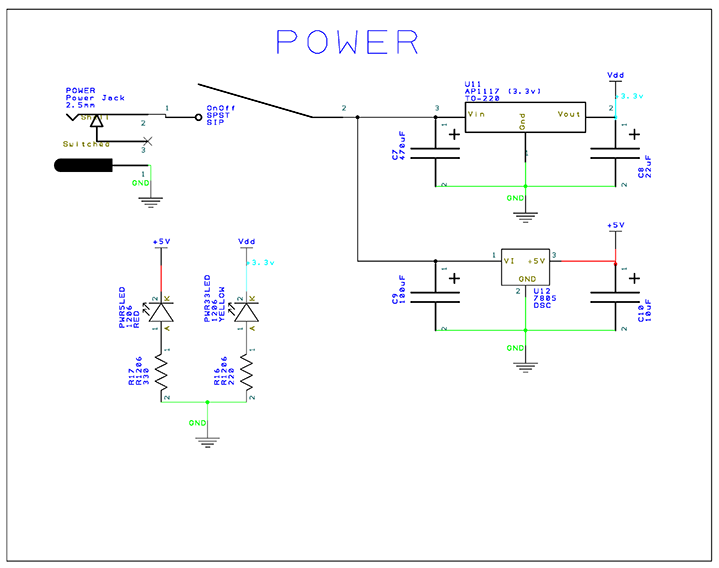
The entire computer is powered by an input of about 7.5 volts, which gets regulated down to 5v and 3.3v. If I built another version of this PCB, I would eliminate the 5V regulation and replace it with an external 5V regulated power supply (wall plug) capable of a few amps, and only generate the 3.3V instead.
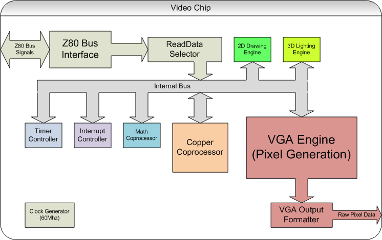
Inside the Video Chip, there is a Z80 Bus Interface module which is responsible for monitoring the state of the various pins that relate to the Z80 Bus. Those signals must be "de-bounced" or "stabilized" by sending each of them through a latch right away. Any logic that attempts to directly make use of those signals without first stabilizing them, risks exhibiting unusual behavior. Because the FPGA is massively parallel, two pieces of FPGA logic may look at the same external signal at a moment of transition, and make a different call as to whether it's a high or a low that is being observed. This was a painful lesson to learn during the debugging phase. Once I stabilized these signals, the chip functioned as the design specified. A second feature of the Z80 Bus Interface is to identify the moment that a Z80 read or write occurs (the moment that triggers it), and turn that external event into an internal event that consumes only a single 60Mhz clock within the remaining FPGA logic. This is important because there is an "Internal Bus" where reads and writes are also occurring, and it must be shared by actions from the external Z80, as well as the internal Copper Video Coprocessor. The Copper will consume all cycles where the Z80 is not active. At 60Mhz, that's most of them. The Z80 probably only generates an internal action once in every 20 or so cycles (worst case), due to the fact that the Z80 is executing at 1/6 the speed, combined with the fact that the Z80 usually executes other instructions between any instruction which DOES happen to interact with the video chip. That works out to about a 5% load from Z80 activity. 95% of the time the Copper is able to do what it wants to do, without waiting for the Z80 to run a cycle, even when the Z80 is hammering the video chip. This same design is true for Z80 reads as well. When the Z80 triggers a read operation, this becomes a single 60mhz read cycle within the FPGA. Obviously, the read-result needs to be latched and offered to the Z80 for a long period of time in order to satisfy Z80 read-timing, but the FPGA can do so without holding a lock on the internal 60Mhz bus. That internal bus is already busy doing whatever else it needs to do again.
The Read Data Selector is a block of code that ultimately took the shape of an Address Decoder. It is responsible for recognizing address regions for all devices internal to the FPGA, and generating the appropriate chip selects, such as the various video registers, the VRAM, etc.
The internal bus is an 8-bit bus (I found that anything larger consumes too many FPGA resources, and is a poor trade). The Internal Bus allows both the Z80 and the Copper to access all other devices. The Z80 gets precedence. The Copper will execute a wait-state if the Z80 happens to be on the bus.
The Timer Controller implements 4 16-bit timers, all of which can produce interrupts. These timers are for the benefit of the Z80. One popular use is to produce 50Hz or 60Hz frequencies for music, or for whatever purpose the programmer sees fit.
The Interrupt Controller is where all interrupt sources come together to produce a master interrupt signal that is sent out on the pin called videoData1_vSyncInt. Before going further, I need to explain that there are two ways the video chip can output an image: 64-color, and 4096-color. The 64-color mode drives the VGA port directly by using several pins of the FPGA. The 4096-color mode is a bunch fancier. It requires a CPLD between the FPGA and the VGA port, which has just enough brains in it to decode some "video data" on its way form the FPGA to the VGA port. In 4096-color mode, each pixel on the screen has 4 clocks, and the CPLD finds 4 bits of color-intensity data for each R,G,B, and also 4 bits of data on the SYNC signal. I don't need 4 bits of granularity on the SYNC signal. But, I can offer extra information, such as both the VSYNC and the VBLANK. So, in 4096 color mode, the Z80 can see the beginning of the VBlank period. But in 64-color mode, the Z80 can only see the beginning of the VSync. When the Z80 receives its' physical interrupt, it can check if any interrupt flags are actually set within the video chip. So with the simpler 64-color daughter card, there is a small performance drawback from the Z80's perspective. In fact, there are two performance hits: If using the 64 color daughter card, you only get the Vertical Sync signal. This is not the same thing as the Vertical Blank signal (which would be the ideal interrupt source). The Vertical Sync is a small pulse that happens WITHIN the larger Vertical Blank phase of image rendering. So, there is a portion of time between when the Vertical Blank begins, and when the Vertical Sync begins, where the Z80 could have been making good use of the VBlank interval. With the limited 64 color daughter card, this time is invisible to the Z80. The 4096 color daughter card overcomes this problem, due to the fact that it's capable of broadcasting all VGA information within its' data stream, and is able to dedicate the videoData1_vSyncInt pin only to producing the best interrupt signal for the CPU. This gives you the maximum performance of triggering an interrupt exactly when the Vertical Blank interval begins.
The Math Coprocessor is implemented as a small collection of registers which can accept input values, and produce output values almost immediately. In fact, only the division and modulo results might take more than one Z80 instruction cycle to execute, but so far, I've not yet seen it happen. Because the Video Chip is clocking so much faster than the Z80, it appears that it can produce a result before the Z80 gets a chance to execute a read instruction to fetch the result, even for multi-cycle division operations.
The Copper Coprocessor (named after the Amiga's COPPER Coprocessor) is a tiny CPU implementation that was inspired by, but is actually quite different from both the COPPER and BLITTER chips found in an Amiga. The intent of this mini-CPU, is to start executing from the top of a small program (automatically restarting on every VBlank). The small program can wait for specific scanlines or even pixels, by using the WAIT instruction, then modify one or more video registers or other bytes of VRAM memory, to create an effect at that position. The simplest of effects might be creating the "copper bar" color effect, where the Copper program would change the background color a little bit on each scanline, creating a rainbow of colors down the screen, often visually exceeding the number of colors that the screen should logically be capable of displaying (e.g. it may be a 16 color image but the copper is making it appear to have thousands of colors by twiddling the background color-register through the entire 4096-color spectrum on each scanline). A more complex program might mess with the vertical or horizontal background scroll values on each scanline, to create a shimmering water effect, or a reflection. It could also move a sprite that rendered already, down below the raster, so that it renders again. The possibilities are limited only by your creativity. The Amiga's COPPER had 3 instructions. My design has 14 instructions, including REPEAT/LOOP, DMA, FILL, SKIP, WAIT, INTERRUPT, and STOP. It is capable of performing similar effects as the Amiga's Copper could, but it can also perform some actions that were associated with the Amiga's BLITTER chip as well (i.e. moving memory around). My computer also has a "bitmapped" graphics mode, and polygons and lines can be rendered into it, but it is not performed by my COPPER processor. Instead, I have a dedicated Drawing Engine (discussed next).
The 2D Drawing Engine is a component that can draw points, lines, rectangles and polygons into a HiColor (bitmapped) background layer, with an optional Stencil Material (more on this later).
The 3D Lighting Engine is a component that can apply some simple 3D lighting to the colors that the 2D Drawing Engine will use (more on this later).
The VGA Engine is where the combining of all Backgrounds, sprites and the HiColor Layer occurs. It is essentially a Compositor. i.e. This is where the final VGA image actually takes form. It ultimately produces a stream of pixel data which is sent to the VGA Output Formatter. This is the heart of the video chip, and will get its' own discussion shortly.
The VGA Output Formatter is responsible for converting the stream of pixel data to something suitable for the chosen Video Daughter Card (64-color or 4096-color) that is currently connected to the computer. i.e. stream 64-color information, or stream 4096-color DAC data. This is also where an artificial scanline effect is (optionally) applied to the image. While scan-doubling vertically (rendering the same scanline twice to convert a 240 scanline tall image into a 480 scanline image), the second row of each scanline may be rendered at half intensity, to produce a CRT Monitor effect.
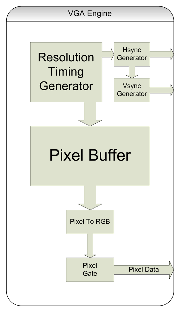
The VGA Resolution Generator is responsible for producing the timing information that produces the desired video signal. i.e. it knows which pixel is being plotted, and how many cycles it is until the next Horizontal or Vertical Sync begins. It drives the HSync and VSync generators, which ultimately produce the HSync and VSync signals. It also informs the Pixel Buffer where we are on the screen at this moment.
The Pixel Buffer is the heart of image generation, so it will be discussed in detail shortly. For now, let's assume that a stream of pixels are coming out of it.
That stream of pixels goes through a Pixel to RGB component, which (in my final implementation) ended up not doing anything. In some designs, this would be a good spot to perform palette lookup to convert to an RGB value. I ended up putting that palette lookup directly in my PixelBuffer implementation.
The Pixel Gate ensures that only black pixels are displayed while in HBlank or VBlank, or else (back in the days of the CRT), you would drag the electron beam across your display to prepare for a new scanline or frame, while accidentally spitting color onto the screen. My implementation does not need a pixel gate.
The FPGA chip only has so much internal RAM, and at some point you need to decide how to partition it and make use of it within your design. I broke it into 4 TileMap Backgrounds, 64 Palettes, 128 Sprites, and a buffer the size of two scanlines. I then dumped the remaining VRAM into a big block of Sprite Image VRAM (amounting to enough VRAM for about 170 sprite images). There is also a HiColor (bitmapped) Background, but it doesn't use any VRAM. Instead, it uses an SDRAM chip (which is attached to the FPGA on the bottom of the Xess FPGA device) as the display ram.
The way the Pixel Buffer works, is to render (produce) a scanline into one of the two scanlines in the Double Buffer, while it pushes the other scanline already present in the Double Buffer out the VGA port at the same time. So, all that matters on each scanline, is that all rendering you WANT to get done, gets done before those two buffers get swapped. Given that we are scan-doubling the display, that actually means we have TWO scanlines of time to produce one scanline of image data! It also means that the ScanBuffer Display Manager must push the same scanline out two times before swapping the buffers.
The 4 TileMap Backgrounds are made up of 8x8 pixel tiles. TileMap Backgrounds are very useful in 8bit computers, because they allow you to avoid having to write each pixel individually. Instead, it only has to write 1 byte to change an entire 8x8 (64-pixel) box on the screen. This is highly desirable on an 8-bit computer because it allows the CPU to update the screen much more rapidly than if it had to write individual pixels. 320x240 pixels is 75K. That's a LOT of data for an 8-bit CPU to move around. In fact, it's more data than the Z80's 64K address space even has! By using a TileMap, you only need to update 40x30 tiles (that's 1.1K instead). A savings of over 90%! The TileMaps also have per-tile palette values. i.e. you can choose a different palette for each tile. Or you can just use the same palette across the entire TileMap. Finally, each TileMap Background has its' own Tile Image Data. TileMap based graphics depend heavily upon re-use of existing tiles across the image. i.e. With a screen full of text, the same letter "A" tile is used repeatedly for every letter A seen on the screen. Of course, the tiles can be any image (or portion of an image), not just a font. And they can use 16 colors within each tile.
The HiColor Layer is a giant frame-buffer of individually accessable pixels, unlike the other TileMap Backgrounds. It accomplishes this, by using a large amount of SDRAM. Because it's SDRAM, however, it requires a periodic refresh (or else it loses track of the data that it contains and the image fades into a bunch of random colors over a few seconds). When a refresh begins, it takes a long time, and can occasionally get in the way of the Z80's attempt to read or write a pixel, so using the Draw Engine to plot one pixel at a time is a rather slow process. You cannot simply read or write a location, you have to set the location and set the value, and then wait for the read or write operation to complete (potentially delayed by a refresh that is currently occurring). All in all, it's a much better idea to use the more complex drawing operations because they can make best use of all available FPGA clock cycles to get the drawing operation completed asap, and they are internally capable of pausing themselves while a refresh occurs. Regarding SDRAM refresh, the system refreshes one row of SDRAM as each scanline begins to draw. All cycles which were not occupied by the refresh or by drawing into the scanbuffer, are made available to the Drawing Engine to produce objects on the screen. The HiColor layer can operate in two modes: 256 colors (1 byte per pixel, paletted) or 4096 colors (2 bytes per pixel, RGB). The Drawing Engine has a 16-bit data bus to the SDRAM so it is not necessarily faster to use the 256-color mode. However, there still is an advantage to using 256 colors: It is paletted. It uses the first 256 color entries of the Palette VRAM, so you can do palette tricks with it, and the Copper CPU can meddle with colors just like it could with TileMaps. One more thing about the HiColor Background: In 4096 color mode, only 12 of the 16 bits are needed for R, G and B. The extra 4 bits can be used for a per-pixel depth option! i.e. you can produce a single image which contains a HUD in the foreground, as well as a full-color backdrop behind the gameplay, and place the sprites and TileMap backgrounds in-between!
The 2D Drawing Engine is a system which can plot points, lines rectangles and polygons. The polygons can be filled or outlined. When pixels are drawn, a solid color can be used or a Material can be assigned. If a material is used, it is rather minimalist, but can produce some classic Stencil effects. It is made up of a 4x4 pixel stencil pattern using 2 colors (This effect is known as 'Stencil Vectors'). The colors can be directly assigned, or can optionally pass through a 3D Lighting Engine before use. The drawing operations can also optionally obey a back-face or front-face cull (Clockwise or Counterclockwise vertex winding). So, although the Drawing Engine is a 2D system (2D vertices), it has some features (Back-face Culling and a Lighting Engine) that can assist in accelerating simple 3D graphics. It also has a Clip Region to clip the drawing operations. "Stencil Vectors" are the act of texturing a 3D polygon in 2D screen-space. It was popular for the short period of time between Solid Color Vectors, and actual 3D Textured Vectors. It gave polygons a textured feel, but the textures would swim around the surface of the model as the object rotated. It was a very unique look. Here is a link to a youtube video containing an example of Stencil Vectors in action (fast forward to 2:20 to see a white cube thing with a bit of a chrome effect on it, followed by a blue and white cube - both of these effects made use of Stencil Vectors, implemented using the BLITTER chip of the Commodore Amiga). My Stencil Vector hardware allows you to either tie the texture position to vertex 0 (so it moves with the object), or tie it to the screen (so it remains static and the surface passes over it as it moves).
The 3D Lighting Engine is a system which can apply some simple 3D lighting calculations against the two drawing colors used by the Drawing Engine. There are two ambient lights. Each ambient light has a color. You can assign one ambient light to both color registers, or assign one to each color register to produce effects such as textures which glow only in certain areas on surfaces). There are also 3 directional lights. Each directional light has a 3D normal indicating the direction that it is shining, and a color of the light. Finally, there is a 3D surface normal which completes the description of the environment for the purposes of lighting. So, all of this works together to give the Z80 the ability to light 3D polygons and environments quickly. Here is a link to a youtube video of an Amiga rotating a cube. Since the Amiga and my computer have the same number of colors, this is a suitable demonstration of what the lighting and drawing engine look like in operation. I have no video of a cube of my own rotating at this time. As you can see, 16 shades per color-gun is surprisingly few, and the color-snapping between intensities can be quite dramatic when an object is rotated slowly, and certainly looks crude when compared to modern computers. Regardless, that's the best you'll get with 4096 colors. Choosing to use bright colors in a dark environment, allows for more shades to be present between the lit and unlit intensities of a surface. Great for space games (check out Elite II: Frontier on the Amiga - a game that made good use of lighting and 3D objects with a 4096-color limit).
The first thing to remember is that this chip is not pushing pixels out to the VGA port the moment they are computed. It is pushing a previously rendered scanline to the VGA port while it spends some time rendering a new scanline to a separate buffer (it has a single scanline back-buffer). So it can take its time and composite several things into a final image of this new scanline, and it is free to paint those pixels in arbitrary order. It also has a fair amount of time to do this, because the FPGA has 4 clocks of time for each pixel, and the entire scanline is also scan-doubled to twice its' height, so there are actually a LOT of clocks per scanline available for producing this composition.
First of all, at the start of every scanline, a time delay is (optionally) respected. This is a programmable time delay that is sometimes useful for allowing the Copper to get in there and setup some video registers. You may want to give a moment for the Copper to setup a complicated video configuration, before beginning to render the scanline. Additionally, a scanline in the HiColor Background Layer is "opened", meaning a small delay is required as the SDRAM prepares to produce the data for us. SDRAM needs to know about a row, column, and page which you intend to access. It takes a bit of time to prepare the result after seeing your request. Once the result is prepared, the SDRAM is ready to stream one pixel per clock, so it will have no trouble keeping up with the rest of the rendering.
The second step, is to render all 4 backgrounds plus the HiColor background, simultaneously. They each provide pixel data, given their current configurations. The background priorities and visibilities are used as a rule to determine which pixel is actually visible. If none of the backgrounds contributed a visible pixel, then the background color from palette#0,Color#0 is used. This pass executes extremely quickly over the entire scanline, and then we have a complete composite of all backgrounds in our buffer.
The third step, is to visit every sprite, checking if it is visible on the current scanline. If it is, then it gets rendered into the scanline at the correct location.
If the scanline runs out of time before all sprites are successfully visited, then any remaining sprites will be omitted from this scanline. In theory it could happen, but I don't see it happening in practice unless I really go out of my way to try to make it happen.
The scanline buffer is made of 28-bit numbers. One for each pixel. That's a strange size. But it has a reason: That's what I need, and the FPGA can do it.
Each pixel contains the following information: 4 bits of red, 4 bits of green, and 4 bits of blue. That's 12 bits already. Next, there is 2 bits of priority information (so that when sprites render, they can determine whether they are above or under the background image or other sprite that has previously been painted here. Next, some sprite-related data is stored: I keep track of an 8-bit SpriteID. This is how the Sprite Collision system detects collisions between specific sprites. There is also a 1-bit flag to indicate whether there was even a sprite here at all! Next, there is a 1-bit value indicating which team the sprite was on when it was rendered here. This allows the collision system to discard collisions between same-team entities (if desired). Finally, 4 bits which indicate presence or absence of each of the BG's. This allows the sprite to collide with a background. These bits are set even if the background itself was set to be invisible. This allows the use of a BG as a collision mask, while never actually seeing it on-screen!
How does the SDRAM get refreshed with reliability? Some scanlines are refreshed automatically for us because they must be visited when they are rendered to the screen. But we cannot rely on that, because not all scanlines of SDRAM are visited. Maybe NONE are, if the background is currently hidden! Or, the COPPER could be doing tricks that cause not all scanlines to be visited (it could mirror the image half way down the screen, for example). So, when the SDRAM is not being used to render a scanline, it is periodically being asked to refresh a very specific region of memory to ensure that all regions are refreshed as required. The timing of these periodic refreshes are setup so that they never conflict with scanline rendering, and are guaranteed to visit all of the SDRAM's useful VRAM address space within the required time-limit. The HiColor address space is the size it is, because it is limited by the refresh algorithm used here. The SDRAM chip is physically larger than the VRAM I offer, but I could not refresh all of it in the time available, and therefore do not give access to all of it either. It's still a half-meg of pixels, more than enough for an 8-bit computer to play with.
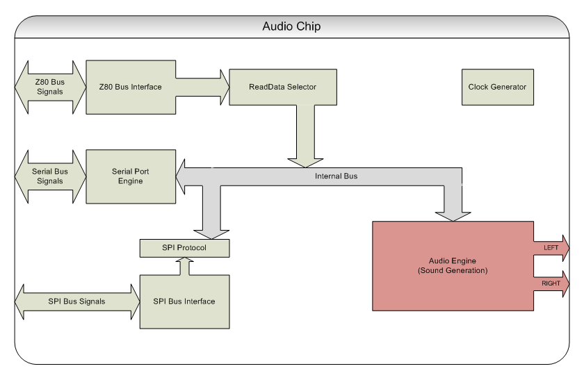
The Audio Chip starts out in a similar pattern to the Video Chip. A Z80 Bus Interface to stabilize and reduce a Z80 read or write operation to a single cycle, and a Read Data Selector which acts similar to an Address Decoder. There's also an Internal Bus, but this time, only the Z80 will make use of it, as there is no coprocessor on this chip.
There is a Serial Port Engine, which implements a simple serial port at 38400 baud, 8N1. This serial port is directly accessible by the Z80 and can be used as a debugging interface, or for whatever purpose you desire.
There is an SPI Protocol layer which is exposed as a small collection of registers to the Z80. By manipulating these registers, the Z80 can initiate data exchanges between the Audio Chip's RAM and the Input Coprocessor which is attached to the same SPI Bus.
The real magic hides within the Audio Engine, which I will discuss next.
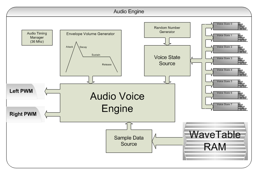
I implemented a hardware Random Number Generator, which is implemented as a 16-bit LFSR (Linear Feedback Shift Register), and chose an initial value which produced the most perfect white noise sound that I could find. This random number source is constantly producing numbers at a rate of 36Mhz, and feeds the 8 voices if they are in "White Noise" mode. The Z80 is also capable of reading random numbers simply by reading a register.
There are 8 voices, all of which need to remember their own state (Their sample start address, length, looping, attack rate, decay rate, etc). Each voice is hard-wired to a specific channel. The Voice State Source is basically a multiplexer that allows the Audio Voice Engine to ask for the state of a specific voice.
There is a big block of RAM where samples can be stored, and the "Sample Data Source" module is able to look-up a specific sample byte, given the state of a specific voice.
There is an Envelope Volume Generator. This module produces an "Envelope Volume" by examining the current state of the voice (specifically, the state of the envelope applied to that voice), and computing the current position within the envelope, and thus the volume that the envelope is applying.
The Audio Voice Engine takes the information from the Envelope, the Voice State, and the Sample Data, to produce a sample. It mixes the samples of 4 voices together to produce the sample to use for each channel. Those samples are then converted to a PWM pulse (one for each channel), and output on the two pins called AudioL and AudioR.
One of the biggest problems is how to deal with changes to the hardware definition. It became very clear to me that the only way to manage this problem, is to create an abstract hardware definition as a text file (I chose Python) and use a tool to convert this definition into headers for various other languages (I generate .H files for C code, .PY files for Python tools, .I files for Assembly code, .VH files for Verilog test suites, and finally, an .HTML version for easier reading). Now, after a hardware change, I usually just have to recompile everything and I'm good to go. Here is a link to a copy of the HTML version, if you wish to browse The Hardware Definition.